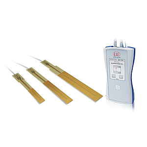

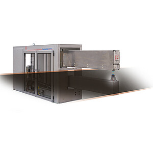
Sensors for semiconductor production
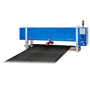
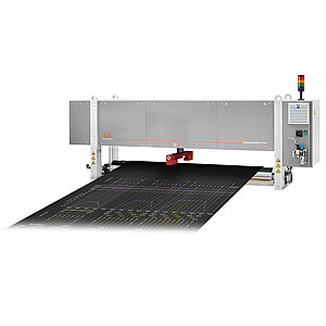
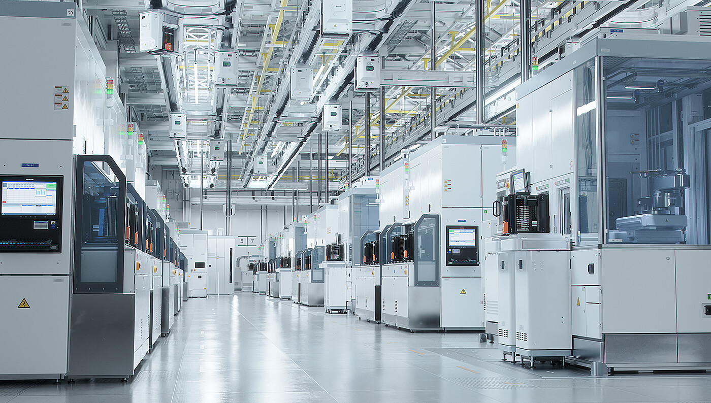
Semiconductor production processes are based on state-of-the-art sensors in order to meet the increasing demands for quality and cost-effectiveness. This means accurately detecting the smallest of movements, reliably identifying when tolerances are exceeded even slightly, and precisely monitoring travel paths. Sensor technologies from Micro-Epsilon have been used by leading manufacturers in the semiconductor industry for many years and impress in front-end processes, back-end applications and in wafer fab automation.

Advantages at a glance:
- High precision sensors - Made in Germany
- Consultation, development & production from a single source
- Customized sensors for series & OEM
- Sensors suitable for clean rooms and vacuums up to UHV
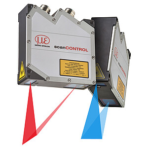
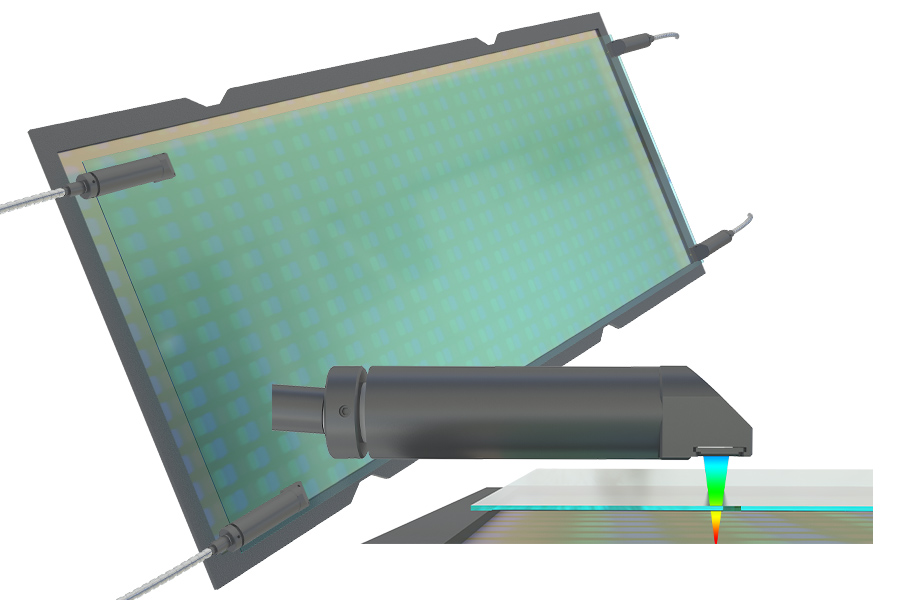
High resolution inspection and positioning of masks
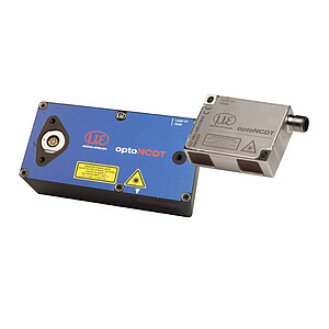
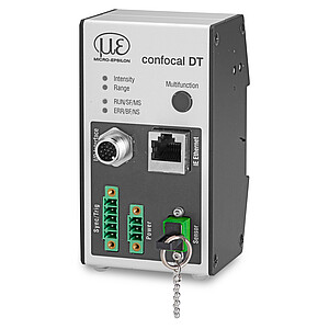
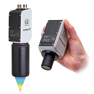
High-resolution and long-term stable measurements of the machine movements must be made when feeding and positioning the lithography mask. For this purpose, high-resolution sensors are used to monitor the mask alignment while meeting nanometer precision requirements. The sensors also monitor the glass and the distance from the carrier. Confocal chromatic sensors detect this gap from only one side.
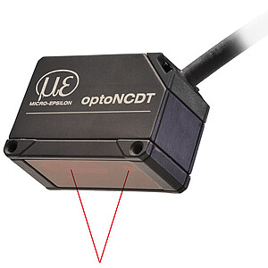
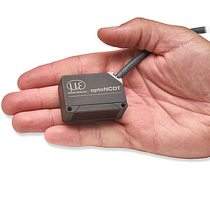
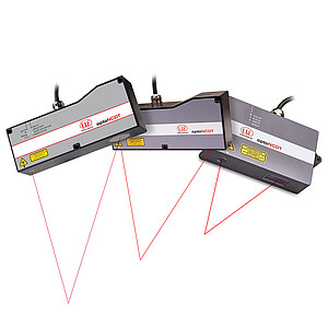
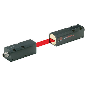
High precision distance measurements in lithography
Wafer lithography - especially EUV lithography - is one of the most complex industrial manufacturing processes. In order to deposit structures in the single-digit nanometer range on the wafer, the machine and optical elements must be positioned and aligned with correspondingly high precision. Sensors from Micro-Epsilon take on a decisive role here: nanometer-precise distance positioning of the lens system and the wafer stages.
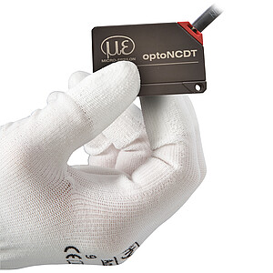
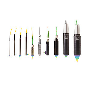
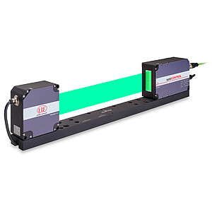
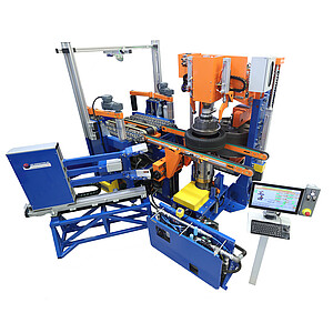
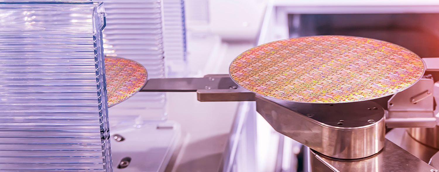
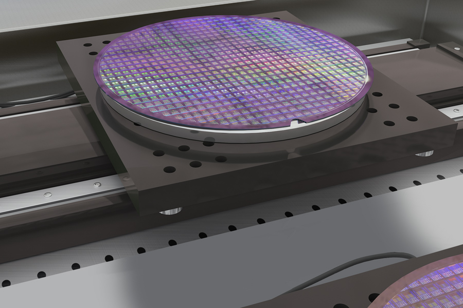
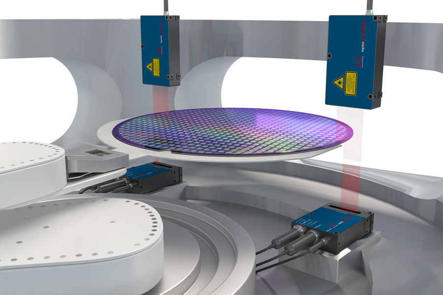
Precise monitoring in wafer handling
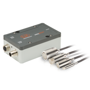
Wafers must be automatically removed and fed to the appropriate processing step throughout the manufacturing process. Accurate positioning is just as important as fast and reliable movement. Sensors from Micro-Epsilon ensure exact alignment and safe transport in every process step. The clean room suitability of the wear-free sensors is a basic requirement for their use. Thanks to the high precision, deviations can be determined quickly and accurately.
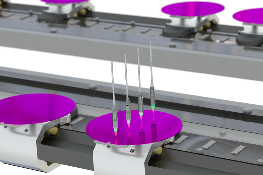
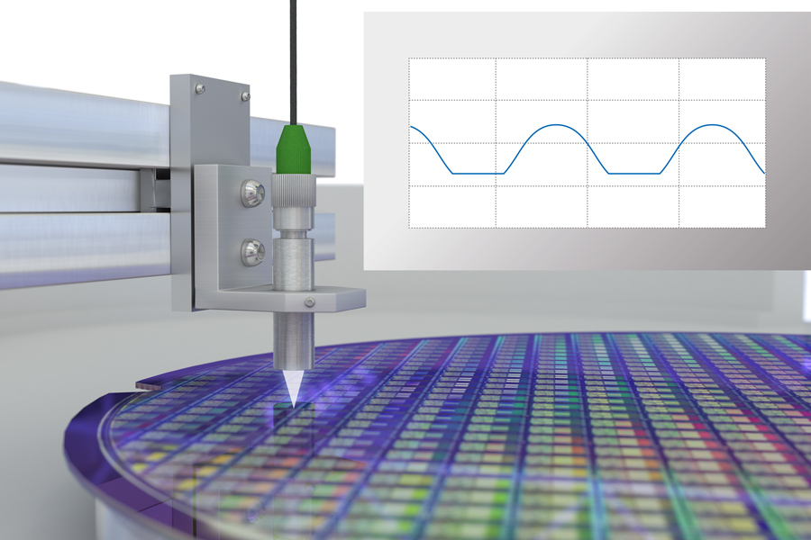
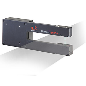
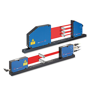
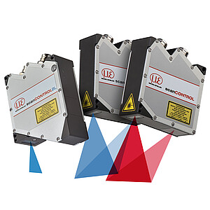
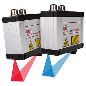
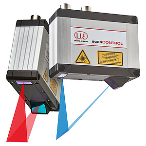
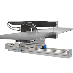
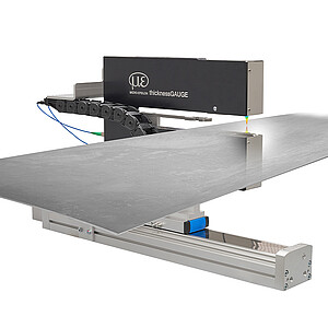
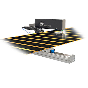
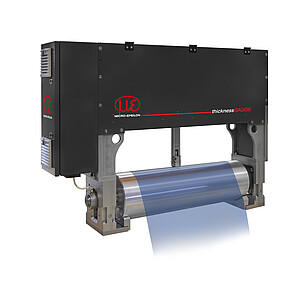
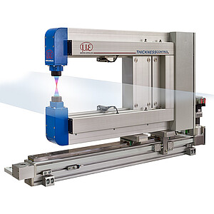
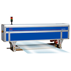
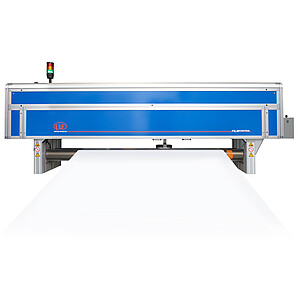
Inline wafer quality control
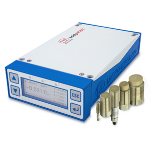
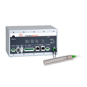
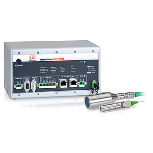
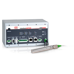
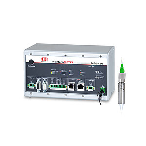
For quality control, sensors from Micro-Epsilon are used in various areas, for example, for testing the coating thickness, for monitoring the deflection as well as separation. In addition to high precision, a high measuring rate is also required to support the high speed manufacturing processes. For example, confocal chromatic sensors are used for one-sided thickness measurement of coatings and height testing of bumps. In other measurement tasks, white light interferometers check the deflection and thickness of wafers with submicrometer accuracy.
Get your white paper now!
Find out how your competitors in the semiconductor industry are already benefiting from modern sensor technology in various fields and thus gaining a clear advantage.
Based on real use cases, we illustrate how you can apply high-performance sensors and measuring systems to reduce error rates and meet the highest accuracy and purity requirements.
Use this white paper to optimize your strategy!